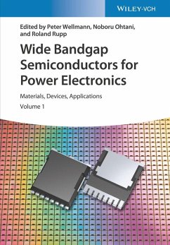
Wide Bandgap Semiconductors for Power Electronics (eBook, PDF)
Materials, Devices, Applications
Redaktion: Wellmann, Peter; Rupp, Roland; Ohtani, Noboru
279,99 €
279,99 €
inkl. MwSt.
Sofort per Download lieferbar

0 °P sammeln
279,99 €
Als Download kaufen

279,99 €
inkl. MwSt.
Sofort per Download lieferbar

0 °P sammeln
Jetzt verschenken
Alle Infos zum eBook verschenken
279,99 €
inkl. MwSt.
Sofort per Download lieferbar
Alle Infos zum eBook verschenken

0 °P sammeln
Wide Bandgap Semiconductors for Power Electronics (eBook, PDF)
Materials, Devices, Applications
Redaktion: Wellmann, Peter; Rupp, Roland; Ohtani, Noboru
- Format: PDF
- Merkliste
- Auf die Merkliste
- Bewerten Bewerten
- Teilen
- Produkt teilen
- Produkterinnerung
- Produkterinnerung

Bitte loggen Sie sich zunächst in Ihr Kundenkonto ein oder registrieren Sie sich bei
bücher.de, um das eBook-Abo tolino select nutzen zu können.
Hier können Sie sich einloggen
Hier können Sie sich einloggen
Sie sind bereits eingeloggt. Klicken Sie auf 2. tolino select Abo, um fortzufahren.

Bitte loggen Sie sich zunächst in Ihr Kundenkonto ein oder registrieren Sie sich bei bücher.de, um das eBook-Abo tolino select nutzen zu können.
The book gives a comprehensive overview the wide bandgap materials SiC, GaN, C (diamond) and Ga(III) oxide, covering in detail the growth of these materials, their characterization and their use in a variety of power electronics devices.
- Geräte: PC
- mit Kopierschutz
- eBook Hilfe
- Größe: 28.33MB
Andere Kunden interessierten sich auch für
![Wide Bandgap Nanowires (eBook, PDF) Wide Bandgap Nanowires (eBook, PDF)]() Tuan Anh PhamWide Bandgap Nanowires (eBook, PDF)142,99 €
Tuan Anh PhamWide Bandgap Nanowires (eBook, PDF)142,99 €![Metal Oxide Semiconductors (eBook, PDF) Metal Oxide Semiconductors (eBook, PDF)]() Zhigang ZangMetal Oxide Semiconductors (eBook, PDF)124,99 €
Zhigang ZangMetal Oxide Semiconductors (eBook, PDF)124,99 €![Composites-Based Perovskite Solar Cells (eBook, PDF) Composites-Based Perovskite Solar Cells (eBook, PDF)]() Yoon-Bong HahnComposites-Based Perovskite Solar Cells (eBook, PDF)124,99 €
Yoon-Bong HahnComposites-Based Perovskite Solar Cells (eBook, PDF)124,99 €![Organic Thermoelectrics (eBook, PDF) Organic Thermoelectrics (eBook, PDF)]() Organic Thermoelectrics (eBook, PDF)142,99 €
Organic Thermoelectrics (eBook, PDF)142,99 €![Semiconductor Electrochemistry (eBook, PDF) Semiconductor Electrochemistry (eBook, PDF)]() Rüdiger MemmingSemiconductor Electrochemistry (eBook, PDF)147,99 €
Rüdiger MemmingSemiconductor Electrochemistry (eBook, PDF)147,99 €![Electronic Processes in Organic Semiconductors (eBook, PDF) Electronic Processes in Organic Semiconductors (eBook, PDF)]() Anna KöhlerElectronic Processes in Organic Semiconductors (eBook, PDF)67,99 €
Anna KöhlerElectronic Processes in Organic Semiconductors (eBook, PDF)67,99 €![Nanotechnology in Electronics (eBook, PDF) Nanotechnology in Electronics (eBook, PDF)]() Nanotechnology in Electronics (eBook, PDF)142,99 €
Nanotechnology in Electronics (eBook, PDF)142,99 €-
-
-
The book gives a comprehensive overview the wide bandgap materials SiC, GaN, C (diamond) and Ga(III) oxide, covering in detail the growth of these materials, their characterization and their use in a variety of power electronics devices.
Dieser Download kann aus rechtlichen Gründen nur mit Rechnungsadresse in A, B, BG, CY, CZ, D, DK, EW, E, FIN, F, GR, HR, H, IRL, I, LT, L, LR, M, NL, PL, P, R, S, SLO, SK ausgeliefert werden.
Produktdetails
- Produktdetails
- Verlag: Wiley-VCH
- Seitenzahl: 736
- Erscheinungstermin: 21. September 2021
- Englisch
- ISBN-13: 9783527824700
- Artikelnr.: 62732701
- Verlag: Wiley-VCH
- Seitenzahl: 736
- Erscheinungstermin: 21. September 2021
- Englisch
- ISBN-13: 9783527824700
- Artikelnr.: 62732701
- Herstellerkennzeichnung Die Herstellerinformationen sind derzeit nicht verfügbar.
Peter Wellmann is Professor at the University of Erlangen-Nuremberg, Germany, and Chair of the Department of Materials for Electronics and Energy Technology. After his PhD he was postdoctoral researcher at the Materials Department of the University of California Santa Barbara, USA. He did his habilitation in Erlangen in 2001 on the topic of vapor growth and characterization of silicon carbide. Peter Wellmann was Visiting Professor at the National Polytechnic Institute of Grenoble and at the University of Montpellier 2, France. Noboru Ohtani is Professor at the School of Science and Technology and Director of the R&D Center for SiC Materials and Processes at Kwansei Gakuin University, Hyogo, Japan. He earned his PhD degree in 1993 from Imperial College London, UK. Prior to joining Kwansei Gakuin University, he worked at the Advanced Technology Research Laboratories of the Nippon Steel Corporation. Roland Rupp is Senior Principal SiC Technology at Infineon AG in Munich, Germany, where he has built up and coordinated the development of SiC technology for power applications. He obtained his Diploma from the University of Erlangen-Nuremberg, and subsequently worked as Research Engineer at Stettner&Co. He then returned to university to obtain his PhD and afterwards worked as Development Engineer at Siemens AG for seven years before taking on his current position.
Introduction
PART I. SILICON CARBIDE (SiC)
Bulk Growth of hex-SiC
Industrial Perspectives on hex-SiC Bulk Growth
CVD Epitaxy of hex-SiC
Industrial Perspective on CVD Epitaxy of hex-SiC
Bulk and Epitaxial Growth of c-SiC
Intrinsic Defects in SiC
Dislocations in SiC Bulk Wafers and Epitaxial Layers: Characterization Using X-Ray Techniques
Dislocations in SiC Bulk Wafers and Epitaxial Layers: Characterization Using Photoluminescence and Two-Photon Absorption Microscopy
Theoretical Approaches to Understanding Evolution and Propagation of Dislocations in SiC
MOS Gate Oxide Interface Defects in SiC
SiC-Graphene Interfaces
Device Processing Using c-SiC and hex-SiC
Unipolar SiC Devices
Bipolar SiC Devices
Reliability of SiC Devices
Industrial Systems Using SiC Circuits
Hybrid Electric Vehicles and Electric Vehicles Applications of SiC
Novel Applications of SiC in Quantum Information
PART II. GALLIUM NITRIDE (GaN), DIAMOND, AND Ga2O3
Ammonothermal and HVPE Bulk Growth of GaN
GaN on Si
HPSG and CVD Growth of Diamond
Diamond Epitaxy and Device Processing
Epitaxial Growth of Beta-Ga2O3
