Ban Wong, Anurag Mittal, Yu Cao, Greg W Starr
Nano-CMOS Circuit and Physical Design
By Ban Wong, Anurag Mittal, Yu Cao et al.
Ban Wong, Anurag Mittal, Yu Cao, Greg W Starr
Nano-CMOS Circuit and Physical Design
By Ban Wong, Anurag Mittal, Yu Cao et al.
- Gebundenes Buch
- Merkliste
- Auf die Merkliste
- Bewerten Bewerten
- Teilen
- Produkt teilen
- Produkterinnerung
- Produkterinnerung
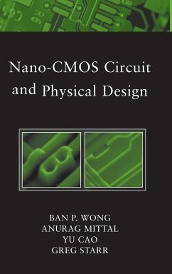
Based on the authors' expansive collection of notes taken over the years, Nano-CMOS Circuit and Physical Design bridges the gap between physical and circuit design and fabrication processing, manufacturability, and yield. This innovative book covers: process technology, including sub-wavelength optical lithography; impact of process scaling on circuit and physical implementation and low power with leaky transistors; and DFM, yield, and the impact of physical implementation.
Andere Kunden interessierten sich auch für
![Low-Voltage Soi CMOS VLSI Devices and Circuits Low-Voltage Soi CMOS VLSI Devices and Circuits]() James B. KuoLow-Voltage Soi CMOS VLSI Devices and Circuits199,99 €
James B. KuoLow-Voltage Soi CMOS VLSI Devices and Circuits199,99 €![Mixed-Signal Systems Mixed-Signal Systems]() Andrzej HandkiewiczMixed-Signal Systems193,99 €
Andrzej HandkiewiczMixed-Signal Systems193,99 €![Nano-CMOS Design for Manufacturability Nano-CMOS Design for Manufacturability]() Ban P. WongNano-CMOS Design for Manufacturability158,99 €
Ban P. WongNano-CMOS Design for Manufacturability158,99 €![Verilog Coding for Logic Synthesis Verilog Coding for Logic Synthesis]() Weng F. LeeVerilog Coding for Logic Synthesis179,99 €
Weng F. LeeVerilog Coding for Logic Synthesis179,99 €![High-Speed VLSI Interconnections High-Speed VLSI Interconnections]() Ashok K GoelHigh-Speed VLSI Interconnections224,99 €
Ashok K GoelHigh-Speed VLSI Interconnections224,99 €![Interconnect Analysis and Synthesis Interconnect Analysis and Synthesis]() Chung-Kuan ChengInterconnect Analysis and Synthesis185,99 €
Chung-Kuan ChengInterconnect Analysis and Synthesis185,99 €![Device Modeling for Analog and RF CMOS Circuit Design Device Modeling for Analog and RF CMOS Circuit Design]() Trond YtterdalDevice Modeling for Analog and RF CMOS Circuit Design202,99 €
Trond YtterdalDevice Modeling for Analog and RF CMOS Circuit Design202,99 €-
-
-
Based on the authors' expansive collection of notes taken over the years, Nano-CMOS Circuit and Physical Design bridges the gap between physical and circuit design and fabrication processing, manufacturability, and yield. This innovative book covers: process technology, including sub-wavelength optical lithography; impact of process scaling on circuit and physical implementation and low power with leaky transistors; and DFM, yield, and the impact of physical implementation.
Hinweis: Dieser Artikel kann nur an eine deutsche Lieferadresse ausgeliefert werden.
Hinweis: Dieser Artikel kann nur an eine deutsche Lieferadresse ausgeliefert werden.
Produktdetails
- Produktdetails
- Verlag: Wiley & Sons
- Artikelnr. des Verlages: 14646610000
- 1. Auflage
- Seitenzahl: 393
- Erscheinungstermin: 1. Dezember 2004
- Deutsch, Englisch
- Abmessung: 240mm x 161mm x 27mm
- Gewicht: 708g
- ISBN-13: 9780471466109
- ISBN-10: 0471466107
- Artikelnr.: 13067594
- Herstellerkennzeichnung
- Libri GmbH
- Europaallee 1
- 36244 Bad Hersfeld
- gpsr@libri.de
Tao Wong is a Canadian author based in Toronto who is best known for his System Apocalypse post-apocalyptic LitRPG series and A Thousand Li, a Chinese xianxia fantasy series. His work has been released in audio, paperback, hardcover and ebook formats and translated into German, Spanish, Portuguese, Russian and other languages. He was shortlisted for the UK Kindle Storyteller award in 2021 for his work, A Thousand Li: the Second Sect.When he's not writing and working, he's practicing martial arts, reading and dreaming up new worlds.Tao became a full-time author in 2019 and is a member of SF Canada, the Science Fiction and Fantasy Writers of America (SFWA) and ALLI.
FOREWORD.
PREFACE.
1 NANO-CMOS SCALING PROBLEMS AND IMPLICATIONS.
1.1 Design Methodology in the Nano-CMOS Era.
1.2 Innovations Needed to Continue Performance Scaling.
1.3 Overview of Sub-100-nm Scaling Challenges and Subwavelength Optical
Lithography.
1.4 Process Control and Reliability.
1.5 Lithographic Issues and Mask Data Explosion.
1.6 New Breed of Circuit and Physical Design Engineers.
1.7 Modeling Challenges.
1.8 Need for Design Methodology Changes.
1.9 Summary.
References.
PART I: PROCESS TECHNOLOGY AND SUBWAVELENGTH OPTICAL LITHOGRAPHY: PHYSICS,
THEORY OF OPERATION, ISSUES, AND SOLUTIONS.
2 CMOS DEVICE AND PROCESS TECHNOLOGY.
2.1 Equipment Requirements for Front-End Processing.
2.2 Front-End-Device Problems in CMOS Scaling.
2.3 Back-End-of-Line Technology.
References.
3 THEORY AND PRACTICALITIES OF SUBWAVELENGTH OPTICAL LITHOGRAPHY.
3.1 Introduction and Simple Imaging Theory.
3.2 Challenges for the 100-nm Node.
3.3 Resolution Enhancement Techniques: Physics.
3.4 Physical Design Style Impact on RET and OPC Complexity.
3.5 The Road Ahead: Future Lithographic Technologies.
References.
PART II: PROCESS SCALING IMPACT ON DESIGN 4 MIXED-SIGNAL CIRCUIT DESIGN.
4.1 Introduction.
4.2 Design Considerations.
4.3 Device Modeling.
4.4 Passive Components.
4.5 Design Methodology.
4.6 Low-Voltage Techniques.
4.7 Design Procedures.
4.8 Electrostatic Discharge Protection.
4.9 Noise Isolation.
4.10 Decoupling.
4.11 Power Busing.
4.12 Integration Problems.
4.13 Summary.
References.
5 ELECTROSTATIC DISCHARGE PROTECTION DESIGN.
5.1 Introduction.
5.2 ESD Standards and Models.
5.3 ESD Protection Design.
5.4 Low-C ESD Protection Design for High-Speed I/O.
5.5 ESD Protection Design for Mixed-Voltage I/O.
5.6 SCR Devices for ESD Protection.
5.7 Summary.
References.
6 INPUT/OUTPUT DESIGN.
6.1 Introduction.
6.2 I/O Standards.
6.3 Signal Transfer.
6.4 ESD Protection.
6.5 I/O Switching Noise.
6.6 Termination.
6.7 Impedance Matching.
6.8 Preemphasis.
6.9 Equalization.
6.10 Conclusion.
References.
7 DRAM.
7.1 Introduction.
7.2 DRAM Basics.
7.3 Scaling the Capacitor.
7.4 Scaling the Array Transistor.
7.5 Scaling the Sense Amplifier.
7.6 Summary.
References.
8 SIGNAL INTEGRITY PROBLEMS IN ON-CHIP INTERCONNECTS.
8.1 Introduction.
8.2 Interconnect Parasitics Extraction.
8.3 Signal Integrity Analysis.
8.4 Design Solutions for Signal Integrity.
8.5 Summary.
References.
9 ULTRALOW POWER CIRCUIT DESIGN.
9.1 Introduction.
9.2 Design-Time Low-Power Techniques.
9.3 Run-Time Low-Power Techniques.
9.4 Technology Innovations for Low-Power Design.
9.5 Perspectives for Future Ultralow-Power Design.
References.
PART III: IMPACT OF PHYSICAL DESIGN ON MANUFACTURING/YIELD AND PERFORMANCE.
10 DESIGN FOR MANUFACTURABILITY.
10.1 Introduction.
10.2 Comparison of Optimal and Suboptimal Layouts.
10.3 Global Route DFM.
10.4 Analog DFM.
10.5 Some Rules of Thumb.
10.6 Summary.
References.
11 DESIGN FOR VARIABILITY.
11.1 Impact of Variations on Future Design.
11.2 Strategies to Mitigate Impact Due to Variations.
11.3 Corner Modeling Methodology for Nano-CMOS Processes.
11.4 New Features of the BSIM4 Model.
11.5 Summary.
References.
INDEX.


