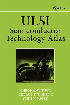
More than 1,100 TEM images illustrate the science of ULSI The natural outgrowth of VLSI (Very Large Scale Integration), Ultra Large Scale Integration (ULSI) refers to semiconductor chips with more than 10 million devices per chip. Written by three renowned pioneers in their field, ULSI Semiconductor Technology Atlas uses examples and TEM (Transmission Electron Microscopy) micrographs to explain and illustrate ULSI process technologies and their associated problems. The first book available on the subject to be illustrated using TEM images, ULSI Semiconductor Technology Atlas is logically divided into four parts: * Part I includes basic introductions to the ULSI process, device construction analysis, and TEM sample preparation * Part II focuses on key ULSI modules--ion implantation and defects, dielectrics and isolation structures, silicides/salicides, and metallization * Part III examines integrated devices, including complete planar DRAM, stacked cell DRAM, and trench cell DRAM, as well as SRAM as examples for process integration and development * Part IV emphasizes special applications, including TEM in advanced failure analysis, TEM in advanced packaging development and UBM (Under Bump Metallization) studies, and high-resolution TEM in microelectronics This innovative guide also provides engineers and managers in the microelectronics industry, as well as graduate students, with: * More than 1,100 TEM images to illustrate the science of ULSI * A historical introduction to the technology as well as coverage of the evolution of basic ULSI process problems and issues * Discussion of TEM in other advanced microelectronics devices and materials, such as flash memories, SOI, SiGe devices, MEMS, and CD-ROMs
Hinweis: Dieser Artikel kann nur an eine deutsche Lieferadresse ausgeliefert werden.
Hinweis: Dieser Artikel kann nur an eine deutsche Lieferadresse ausgeliefert werden.

