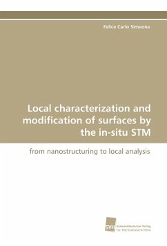
The need of a deep comprehension at an atomic level of phenomena occurring a the electrified interface, pushed the scientific community to develop methods for the modification and characterization of active surfaces with atomic spacial resolution. The Scanning Tunneling Microscopy (STM) is playing a pivotal role in this challenge, allowing for the detailed analysis of the morphology and, a the same time, for the nano-scale modification of the substrate, opening the road to one of the most active field of contemporary research: nano-technology. In this field, the Electrochemical-STM (EC-STM) has emerged as a powerful tool for the controlled nanostructuring of electrode surfaces, due to its unique capability of operating at room conditions of pressure and temperature. Moreover, the analysis of the current flowing through the STM gap operating under electrochemical control, yealds detailed informations on the "local" structure and electronic properties of the interface.
Bitte wählen Sie Ihr Anliegen aus.
Rechnungen
Retourenschein anfordern
Bestellstatus
Storno

