Nicolas Brodusch, Hendrix Demers, Raynald Gauvin
Field Emission Scanning Electron Microscopy
New Perspectives for Materials Characterization
Nicolas Brodusch, Hendrix Demers, Raynald Gauvin
Field Emission Scanning Electron Microscopy
New Perspectives for Materials Characterization
- Broschiertes Buch
- Merkliste
- Auf die Merkliste
- Bewerten Bewerten
- Teilen
- Produkt teilen
- Produkterinnerung
- Produkterinnerung
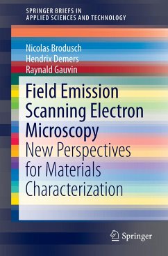
This book highlights what is now achievable in terms of materials characterization with the new generation of cold-field emission scanning electron microscopes applied to real materials at high spatial resolution. It discusses advanced scanning electron microscopes/scanning- transmission electron microscopes (SEM/STEM), simulation and post-processing techniques at high spatial resolution in the fields of nanomaterials, metallurgy, geology, and more. These microscopes now offer improved performance at very low landing voltage and high -beam probe current stability, combined with a routine…mehr
Andere Kunden interessierten sich auch für
![Scanning Electron Microscopy and X-Ray Microanalysis Scanning Electron Microscopy and X-Ray Microanalysis]() Joseph I. GoldsteinScanning Electron Microscopy and X-Ray Microanalysis86,99 €
Joseph I. GoldsteinScanning Electron Microscopy and X-Ray Microanalysis86,99 €![Physical Principles of Electron Microscopy Physical Principles of Electron Microscopy]() R. F. EgertonPhysical Principles of Electron Microscopy70,99 €
R. F. EgertonPhysical Principles of Electron Microscopy70,99 €![Electron Microdiffraction Electron Microdiffraction]() J. M. ZuoElectron Microdiffraction121,99 €
J. M. ZuoElectron Microdiffraction121,99 €![Biological Field Emission Scanning Electron Microscopy, 2 Volume Set Biological Field Emission Scanning Electron Microscopy, 2 Volume Set]() Biological Field Emission Scanning Electron Microscopy, 2 Volume Set225,99 €
Biological Field Emission Scanning Electron Microscopy, 2 Volume Set225,99 €![2nd International Multidisciplinary Microscopy and Microanalysis Congress 2nd International Multidisciplinary Microscopy and Microanalysis Congress]() 2nd International Multidisciplinary Microscopy and Microanalysis Congress116,99 €
2nd International Multidisciplinary Microscopy and Microanalysis Congress116,99 €![3rd International Multidisciplinary Microscopy and Microanalysis Congress (InterM) 3rd International Multidisciplinary Microscopy and Microanalysis Congress (InterM)]() 3rd International Multidisciplinary Microscopy and Microanalysis Congress (InterM)116,99 €
3rd International Multidisciplinary Microscopy and Microanalysis Congress (InterM)116,99 €![Ordering Phenomena in Rare-Earth Nickelate Heterostructures Ordering Phenomena in Rare-Earth Nickelate Heterostructures]() Matthias HeptingOrdering Phenomena in Rare-Earth Nickelate Heterostructures77,99 €
Matthias HeptingOrdering Phenomena in Rare-Earth Nickelate Heterostructures77,99 €-
-
-
This book highlights what is now achievable in terms of materials characterization with the new generation of cold-field emission scanning electron microscopes applied to real materials at high spatial resolution. It discusses advanced scanning electron microscopes/scanning- transmission electron microscopes (SEM/STEM), simulation and post-processing techniques at high spatial resolution in the fields of nanomaterials, metallurgy, geology, and more. These microscopes now offer improved performance at very low landing voltage and high -beam probe current stability, combined with a routine transmission mode capability that can compete with the (scanning-) transmission electron microscopes (STEM/-TEM) historically run at higher beam accelerating voltage
Produktdetails
- Produktdetails
- SpringerBriefs in Applied Sciences and Technology
- Verlag: Springer / Springer Nature Singapore / Springer, Berlin
- Artikelnr. des Verlages: 978-981-10-4432-8
- 1st ed. 2018
- Seitenzahl: 152
- Erscheinungstermin: 6. Oktober 2017
- Englisch
- Abmessung: 235mm x 155mm x 9mm
- Gewicht: 256g
- ISBN-13: 9789811044328
- ISBN-10: 9811044325
- Artikelnr.: 47731060
- Herstellerkennzeichnung Die Herstellerinformationen sind derzeit nicht verfügbar.
Mr. Nicolas Brodusch is the Chief Electron Microscopist in the material engineering department at McGill University, Canada since 2010. He graduated at the Université Paris-Sud, Orsay, France in Material Engineering in 1997. Involved in the field of electron microscopies since 2007, he is research interested in developing and improving new scanning electron microscopy techniques to push the limits of imaging and analysis in the field of materials science and nanomaterials. He is a world leader in diffraction and transmission techniques in the scanning electron microscope. He was awarded in 2014 for the Best Techniques and Instrumentation Development paper for year 2013 in the Microscopy and Microanalysis journal. Dr. Hendrix Demers is a Research Associate in material engineering department at McGill University, Montreal, Canada since 2012. He received his PhD in Mining and Materials Engineering at the McGill University, Montreal, Canada in 2008. He is involved in the field of microscopy and microanalysis by developing new methods for quantitative x-ray microanalysis, for materials characterization, and data and image analysis. He is also author and co-author of a world-renowned research softwares (Win X-Ray, MC X-ray, and CASINO) and aims at helping SEM users in their X-ray microanalyses, metrology applications and in more advanced applications such as electron beam lithography. He won the Castaing Award in 2008 for the best student paper and the Heinrich Award in 2010 for the Outstanding Young Scientist from the Microbeam Analysis Society of America. He is also an Academic Editor of the Scanning journal. Prof. Raynald Gauvin is full Professor at McGill University, Montréal, Canada. His research interest are related in developing new methods to characterize the microstructure of materials using high resolution scanning electron microscopy with x-ray microanalysis and Monte Carlo simulations. He is the creator of the CASINO program that is used by morethan 10 000 users in the world. He has more than 300 papers in scientific journals and conference proceedings. He was Invited Speaker in more than 100 international scientific conferences. He won several scientific prices, most notably the 31st Canadian Materials Physics Medal in 2007 by the Metallurgical Society of the Canadian Institute of Mining, the Heinrich Award in 1997 from the Microbeam Analysis Society of America and the Prix d'excellence du Président de l'École for the best Doctorate Thesis defended in 1990 at l'École Polytechnique de Montréal. Pr. Gauvin was the President of the Inter American Societies of Electron Microscopy (CIASEM) from 2009 to 2011, the President of the Microbeam Analysis Society of America (MAS) from 2005 to 2006, the President of the Microscopical Society of Canada (SMC) from 2001 to 2003 and the President of the International Union of the Microbeam Analysis Societies (IUMAS) from 2000 to 2005. He is currently the holder of the Birks Chair in Metallurgy.
1. Introduction
2. Developments in field emission gun technologies and advanced detection
systems
3. Advanced specimen preparation
a. Surface preparation
b. Surface cleaning
c. Charging compensation with ionic liquid treatment
4. Electron detection strategies for high resolution imaging: Deceleration
and energy filtration
a. Principles
b. Application of dual in-lens electron detection
c. Energy filtration
5. Low voltage SEM
a. Strategy of characterization: deceleration and energy filtration
b. High resolution imaging
c. Low voltage, specimen charging and material contrast
d. Ultra-low voltage SEM: uses and limitations
6. Low voltage STEM in the SEM
7. X-ray imaging
a. X-ray imaging with a large solid angle annular silicon drift detector
b. Material science applications: Mapping at high resolution with high
signal-to-noise ratio
c. The f-ratio method for quantitative x-ray analysis
8. Electron diffraction techniques in the SEM
b. Low voltage STEM defects Imaging
c. Electron Backscatter Diffraction
d. Dark-Field Electron Backscatter Diffraction
e. Transmission Forward Electron Backscatter Diffraction
f. Dark-Field Imaging with a Forecaster Detector in Transmission Mode
9. Magnetic domain imaging
10. General conclusion and perspectives

