Won Y Yang, Taeho Im, Jaekwon Kim, Kyung W Park, Donghyun Baek, Sungjoon Lim, Jingon Joung, Suhyun Park, Han L Lee, Woo June Choi
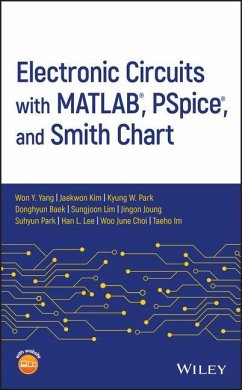
Electronic Circuits with Matlab, Pspice, and Smith Chart
Won Y Yang, Taeho Im, Jaekwon Kim, Kyung W Park, Donghyun Baek, Sungjoon Lim, Jingon Joung, Suhyun Park, Han L Lee, Woo June Choi
Electronic Circuits with Matlab, Pspice, and Smith Chart
- Gebundenes Buch
Andere Kunden interessierten sich auch für
![Digital Signal and Image Processing Using Matlab, Volume 3 Digital Signal and Image Processing Using Matlab, Volume 3]() Gérard BlanchetDigital Signal and Image Processing Using Matlab, Volume 3192,99 €
Gérard BlanchetDigital Signal and Image Processing Using Matlab, Volume 3192,99 €![Smart Antennas with Matlab, Second Edition Smart Antennas with Matlab, Second Edition]() Frank GrossSmart Antennas with Matlab, Second Edition172,99 €
Frank GrossSmart Antennas with Matlab, Second Edition172,99 €![Digital Signal and Image Processing Using Matlab, Volume 2 Digital Signal and Image Processing Using Matlab, Volume 2]() Gérard BlanchetDigital Signal and Image Processing Using Matlab, Volume 2191,99 €
Gérard BlanchetDigital Signal and Image Processing Using Matlab, Volume 2191,99 €![Otto J. M. Smith Otto J. M. Smith]() Otto J. M. Smith32,99 €
Otto J. M. Smith32,99 €![Digital Signal and Image Processing Using Matlab, Volume 1 Digital Signal and Image Processing Using Matlab, Volume 1]() Gérard BlanchetDigital Signal and Image Processing Using Matlab, Volume 1228,99 €
Gérard BlanchetDigital Signal and Image Processing Using Matlab, Volume 1228,99 €![Cooling Techniques for Electronic Equipment Cooling Techniques for Electronic Equipment]() Dave S SteinbergCooling Techniques for Electronic Equipment320,99 €
Dave S SteinbergCooling Techniques for Electronic Equipment320,99 €![Electronic and Photonic Circuits and Devices Electronic and Photonic Circuits and Devices]() Electronic and Photonic Circuits and Devices197,99 €
Electronic and Photonic Circuits and Devices197,99 €-
-
-
Produktdetails
- Verlag: Wiley
- Seitenzahl: 880
- Erscheinungstermin: 15. Januar 2020
- Englisch
- Abmessung: 231mm x 155mm x 36mm
- Gewicht: 1139g
- ISBN-13: 9781119598923
- ISBN-10: 1119598923
- Artikelnr.: 56712910
Hinweis: Dieser Artikel kann nur an eine deutsche Lieferadresse ausgeliefert werden.
- Herstellerkennzeichnung
- Libri GmbH
- Europaallee 1
- 36244 Bad Hersfeld
- gpsr@libri.de
Won Y. Yang, PhD, is an Emeritus Professor in the Department of Electrical Engineering at Chung-Ang University in Seoul, Korea. Jaekwon Kim, PhD, is a Professor in the Department of Computer & Telecommunications Engineering at Yonsei University in Wonju, Korea. Kyung W. Park, PhD, is a Managerial Researcher at Korea Electronics Technology Institute, Seoul, Korea. Donghyun Baek, PHD, is a Professor in the Department of Electrical Engineering at Chung-Ang University in Seoul, Korea. Sungjoon Lim, PhD, is a Professor in the Department of Electrical Engineering at Chung-Ang University in Seoul, Korea. Jingon Joung, PhD, is a Professor in the Department of Electrical Engineering at Chung-Ang University in Seoul, Korea. Suhyun Park, PhD, is a Professor in the Department of Electrical Engineering at Chung-Ang University in Seoul, Korea. Han L. Lee, PhD, is a Professor in the Department of Electrical Engineering at Chung-Ang University in Seoul, Korea. Woo June Choi, PhD, is a Professor in the Department of Electrical Engineering at Chung-Ang University in Seoul, Korea. Taeho Im, PhD, is a Professor in Oceanic IT Engineering at Hoseo University in Asan, Korea.
Preface xiii
About the Companion Website xv
1 Load Line Analysis and Fourier Series 1
1.1 Load Line Analysis 1
1.1.1 Load Line Analysis of a Nonlinear Resistor Circuit 3
1.1.2 Load Line Analysis of a Nonlinear RL circuit 7
1.2 Voltage-Current Source Transformation 10
1.3 Thevenin/Norton Equivalent Circuits 11
1.4 Miller's Theorem 18
1.5 Fourier Series 18
1.5.1 Computation of Fourier Coefficients Using Symmetry 20
1.5.2 Circuit Analysis Using Fourier Series 29
1.5.3 RMS Value and Distortion Factor of a Non-Sinusoidal Periodic Signal
35
Problems 36
2 Diode Circuits 43
2.1 The v-i Characteristic of Diodes 43
2.1.1 Large-Signal Diode Model for Switching Operations 44
2.1.2 Small-Signal Diode Model for Amplifying Operations 44
2.2 Analysis/Simulation of Diode Circuits 46
2.2.1 Examples of Diode Circuits 46
2.2.2 Clipper/Clamper Circuits 51
2.2.3 Half-wave Rectifier 53
2.2.4 Half-wave Rectifier with Capacitor - Peak Rectifier 53
2.2.5 Full-wave Rectifier 57
2.2.6 Full-wave Rectifier with LC Filter 59
2.2.7 Precision Rectifiers 62
2.2.7.1 Improved Precision Half-wave Rectifier 63
2.2.7.2 Precision Full-wave Rectifier 65
2.2.8 Small-Signal (AC) Analysis of Diode Circuits 67
2.3 Zender Diodes 75
Problems 85
3 BJT Circuits 105
3.1 BJT (Bipolar Junction Transistor) 106
3.1.1 Ebers-Moll Representation of BJT 106
3.1.2 Operation Modes (Regions) of BJT 109
3.1.3 Parameters of BJT 109
3.1.4 Common-Base Configuration 111
3.1.5 Common-Emitter Configuration 113
3.1.6 Large-Signal (DC) Model of BJT 115
3.1.7 Small-Signal (AC) Model of BJT 142
3.1.8 Analysis of BJT Circuits 143
3.1.9 BJT Current Mirror 156
3.1.10 BJT Inverter/Switch 161
3.1.11 Emitter-Coupled Differential Pair 165
3.2 BJT Amplifier Circuits 168
3.2.1 Common-Emitter (CE) Amplifier 169
3.2.2 Common-Collector (CC) Amplifier (Emitter Follower) 173
3.2.3 Common-Base (CB) Amplifier 180
3.2.4 Multistage Cascaded BJT Amplifier 187
3.2.5 Composite/Compound Multi-Stage BJT Amplifier 199
3.3 Logic Gates Using Diodes/Transistors[C-3, M-1] 209
3.3.1 DTL NAND Gate 209
3.3.2 TTL NAND Gate 215
3.3.2.1 Basic TTL NAND Gate Using Two BJTs 215
3.3.2.2 TTL NAND Gate Using Three BJTs 218
3.3.2.3 Totem-Pole Output Stage 222
3.3.2.4 Open-Collector Output and Tristate Output 227
3.3.3 ECL (Emitter-Coupled Logic) OR/NOR Gate 229
3.4 Design of BJT Amplifier 239
3.4.1 Design of CE Amplifier with Specified Voltage Gain 232
3.4.2 Design of CC Amplifier (Emitter Follower) with Specified Input
Resistance 239
3.5 BJT Amplifier Frequency Response 243
3.5.1 CE Amplifier 243
3.5.2 CC Amplifier (Emitter Follower) 248
3.5.3 CB Amplifier 255
3.6 BJT Inverter Time Response 259
Problems 266
4 FET Circuits 303
4.1 Field-Effect Transistor (FET) 303
4.1.1 JFET (Junction FET) 304
4.1.2 MOSFET (Metal-Oxide-Semiconductor FET) 313
4.1.3 MOSFET Used as a Resistor 327
4.1.4 FET Current Mirror 328
4.1.5 MOSFET Inverter 338
4.1.5.1 NMOS Inverter Using an Enhancement NMOS as a Load 342
4.1.5.2 NMOS Inverter Using a Depletion NMOS as a Load 347
4.1.5.3 CMOS Inverter 350
4.1.6 Source-Coupled Differential Pair 355
4.1.7 CMOS Logic Circuits 359
4.2 FET Amplifer 360
4.2.1 Common-Source (CS) Amplifier 362
4.2.2 CD Amplifier (Source Follower) 366
4.2.3 Common-Gate (CG) Amplifier 370
4.2.4 Common-Source (CS) Amplifier with FET Load 373
4.2.4.1 CS Amplifier with an Enhancement FET Load 373
4.2.4.2 CS Amplifier with a Depletion FET Load 376
4.2.5 Multistage FET Amplifiers 380
4.3 Design of FET Amplifier 398
4.3.1 Design of CS Amplifier 398
4.3.2 Design of CD Amplifier 405
4.4 FET Amplifier Frequency Response 409
4.4.1 CS Amplifier 410
4.4.2 CD Amplifier (Source Follower) 415
4.4.3 CG Amplifier 419
4.5 FET Inverter Time Response 423
Problems 428
5 OP Amp Circuits 467
5.1 OP Amp Basics[Y-1] 468
5.2 OP Amp Circuits with Resistors[Y-1] 471
5.2.1 OP Amp Circuits with Negative Feedback 471
5.2.1.1 Inverting OP Amp Circuit 471
5.2.1.2 Non-Inverting OP Amp Circuit 473
5.2.1.3 Voltage Follower 476
5.2.1.4 Linear Combiner 477
5.2.2 OP Amp Circuits with Positive Feedback 479
5.2.2.1 Inverting Positive Feedback OP Amp Circuit 480
5.2.2.2 Non-Inverting Positive Feedback OP Amp Circuit 481
5.3 First-Order OP Amp Circuits[Y-1] 485
5.3.1 First-Order OP Amp Circuits with Negative Feedback 485
5.3.2 First-Order OP Amp Circuits with Positive Feedback 487
5.3.2.1 Square(Rectangular)-Wave Generator 487
5.3.2.2 Rectangular/Triangular-Wave Generator 490
5.3.3 555 Timer Using OP Amp as Comparator 492
5.4 Second-Order OP Amp Circuits[Y-1] 495
5.4.1 MFB (Multi-FeedBack) Topology 495
5.4.2 Sallen-Key Topology 496
5.5 Active Filter[Y-1] 502
5.5.1 First-Order Active Filter 502
5.5.2 Second-Order Active LPF/HPF 503
5.5.3 Second-Order Active BPF 505
5.5.4 Second-Order Active BSF 507
Problems 512
6 Analog Filter 523
6.1 Analog Filter Design 523
6.2 Passive Filter 533
6.2.1 Low-pass Filter (LPF) 533
6.2.1.1 Series LR Circuit 533
6.2.1.2 Series RC Circuit 535
6.2.2 High-pass Filter (HPF) 535
6.2.2.1 Series CR Circuit 535
6.2.2.2 Series RL Circuit 536
6.2.3 Band-pass Filter (BPF) 537
6.2.3.1 Series Resistor, an Inductor, and a Capacitor (RLC) Circuit and
Series Resonance 536
6.2.3.2 Parallel RLC Circuit and Parallel Resonance 539
6.2.4 Band-stop Filter (BSF) 541
6.2.4.1 Series RLC Circuit 541
6.2.4.2 Parallel RLC Circuit 544
6.2.5 Quality Factor 545
6.2.6 Insertion Loss 549
6.2.7 Frequency Scaling and Transformation 549
6.3 Passive Filter Realization 553
6.3.1 LC Ladder 553
6.3.2 L-Type Impedance Matcher 561
6.3.3 T- and ¿-Type Impedance Matchers 565
6.3.4 Tapped-C Impedance Matchers 571
6.4 Active Filter Realization 576
Problems 586
7 Smith Chart and Impedance Matching 601
7.1 Transmission Line 601
7.2 Smith Chart 608
7.3 Impedance Matching Using Smith Chart 616
7.3.1 Reactance Effect of a Lossless Line 616
7.3.2 Single-Stub Impedance Matching 618
7.3.2.1 Shunt-Connected Single Stub 618
7.3.2.2 Series-Connected Single Stub 622
7.3.3 Double-Stub Impedance Matching 626
7.3.4 The Quarter-Wave Transformer 631
7.3.4.1 Binomial Multisection QWT 633
7.3.4.2 Chebyshev Multisection QWT 634
7.3.5 Filter Implementation Using Stubs[P-1] 635
7.3.6 Impedance Matching with Lumped Elements 646
Problems 661
8 Two-Port Network and Parameters 677
8.1 Two-Port Parameters[Y-1] 677
8.1.1 Definitions and Examples of Two-Port Parameters 678
8.1.2 Relationships Among Two-Port Parameters 685
8.1.3 Interconnection of Two-Port Networks 689
8.1.3.1 Series Connection and z-parameters 690
8.1.3.2 Parallel (Shunt) Connection and y-parameters 690
8.1.3.3 Series-Parallel(Shunt) Connection and h-parameters 691
8.1.3.4 Parallel(Shunt)-Series Connection and g-parameters 691
8.1.3.5 Cascade Connection and a-parameters 692
8.1.4 Curse of Port Condition 692
8.1.5 Circuit Models with Given Parameters 697
8.1.5.1 Circuit Model with Given z-parameters 697
8.1.5.2 Circuit Model with Given y-parameters 699
8.1.5.3 Circuit Model with Given a/b-parameters 699
8.1.5.4 Circuit Model with Given h/g-parameters 699
8.1.6 Properties of Two-Port Networks with Source/Load 700
8.2 Scattering Parameters 709
8.2.1 Definition of Scattering Parameters 709
8.2.2 Two-Port Network with Source/Load 714
8.3 Gain and Stability 723
8.3.1 Two-Port Power Gains[L-1, P-1] 723
8.3.2 Stability[E-1, L-1, P-1] 728
8.3.3 Design for Maximum Gain[M-2, P-1] 733
8.3.4 Design for Specified Gain[M-2, P-1] 740
Problems 746
Appendix A Laplace Transform 761
Appendix B Matrix Operations with MATLAB 767
Appendix C Complex Number Operations with MATLAB 773
Appendix D Nonlinear/Differential Equations with MATLAB 775
Appendix E Symbolic Computations with MATLAB 779
Appendix F Useful Formulas 783
Appendix G Standard Values of Resistors, Capacitors, and Inductors 785
Appendix H OrCAD/PSpice® 791
Appendix I MATLAB® Introduction 831
Appendix J Diode/BJT/FET 835
Bibliography 845
Index 849

