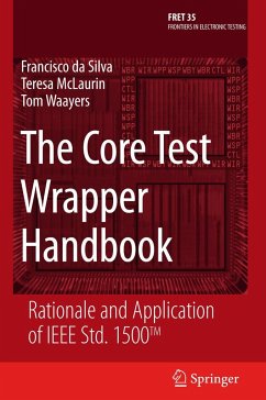
In the early to mid-1990's while working at what was then Motorola Se- conductor, business changes forced my multi-hundred dollar microprocessor to become a tens-of-dollars embedded core. I ran into first hand the problem of trying to deliver what used to be a whole chip with something on the order of over 400 interconnect signals to a design team that was going to stuff it into a package with less than 220 signal pins and surround it with other logic. I also ran into the problem of delivering microprocessor specification verifi- tion - a microprocessor is not just about the functions and instructions included with the instruction set, but also the MIPs rating at some given f- quency. I faced two dilemmas: one, I could not deliver functional vectors without significant development of off-core logic to deal with the reduced chip I/O map (and everybody's I/O map was going to be a little different); and two, the JTAG (1149. 1) boundary scan ring that was around my core when it was achip was going to be woefully inadequate since it did not support - speed signal application and capture and independent use separate from my core. I considered the problem at length and came up with my own solution that was predominantly a separate non-JTAG scan test wrapper that supported at-speed application of launch-capture cycles using the system clock. But my problems weren't over at that point either.
Hinweis: Dieser Artikel kann nur an eine deutsche Lieferadresse ausgeliefert werden.
Hinweis: Dieser Artikel kann nur an eine deutsche Lieferadresse ausgeliefert werden.


