Schade – dieser Artikel ist leider ausverkauft. Sobald wir wissen, ob und wann der Artikel wieder verfügbar ist, informieren wir Sie an dieser Stelle.
  • Format: PDF

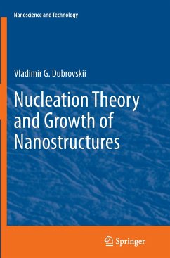
Semiconductor nanostructures such as nanowires are promising building blocks of future nanoelectronic, nanophotonic and nanosensing devices. Their physical properties are primarily determined by the epitaxy process which is rather different from the conventional thin film growth. This book shows how the advanced nucleation theory can be used in modeling of growth properties, morphology and crystal phase of such nanostructures. The book represents a systematic account of modern nucleation theory in open systems, nanostructure nucleation and growth mechanisms, and possibilities for tuning the nanostructure properties to the desired values.…mehr

Produktbeschreibung
Semiconductor nanostructures such as nanowires are promising building blocks of future nanoelectronic, nanophotonic and nanosensing devices. Their physical properties are primarily determined by the epitaxy process which is rather different from the conventional thin film growth. This book shows how the advanced nucleation theory can be used in modeling of growth properties, morphology and crystal phase of such nanostructures. The book represents a systematic account of modern nucleation theory in open systems, nanostructure nucleation and growth mechanisms, and possibilities for tuning the nanostructure properties to the desired values.
Autorenporträt
Head of the Department of theoretical physics
Deputy Director of Nanotechnology Centre
Head of the Laboratory of physics of nanostructures
Coordinator of Associated International Laboratory “Nanostructures of compound semiconductors, Growth, Properties, Devices” (ILNACS)
Deputy Director of Russian-Chinese joint laboratory “Zh.I. Alferov laboratory of information optoelectronics and nanoheterostructures”