53,95 €
53,95 €
inkl. MwSt.
Sofort per Download lieferbar
payback
27 °P sammeln
53,95 €
53,95 €
inkl. MwSt.
Sofort per Download lieferbar

Alle Infos zum eBook verschenken
payback
27 °P sammeln
Als Download kaufen
53,95 €
inkl. MwSt.
Sofort per Download lieferbar
payback
27 °P sammeln
Jetzt verschenken
53,95 €
inkl. MwSt.
Sofort per Download lieferbar

Alle Infos zum eBook verschenken
payback
27 °P sammeln
  • Format: ePub

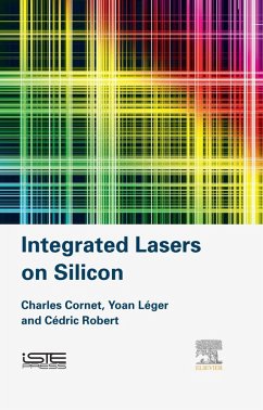
Integrated Lasers on Silicon provides a comprehensive overview of the state-of-the-art use of lasers on silicon for photonic integration. The authors demonstrate the need for efficient laser sources on silicon, motivated by the development of on-board/on-chip optical interconnects and the different integration schemes available. The authors include detailed descriptions of Group IV-based lasers, followed by a presentation of the results obtained through the bonding approach (hybrid III-V lasers). The monolithic integration of III-V semiconductor lasers are explored, concluding with a…mehr

Produktbeschreibung
Integrated Lasers on Silicon provides a comprehensive overview of the state-of-the-art use of lasers on silicon for photonic integration. The authors demonstrate the need for efficient laser sources on silicon, motivated by the development of on-board/on-chip optical interconnects and the different integration schemes available. The authors include detailed descriptions of Group IV-based lasers, followed by a presentation of the results obtained through the bonding approach (hybrid III-V lasers). The monolithic integration of III-V semiconductor lasers are explored, concluding with a discussion of the different kinds of cavity geometries benchmarked with respect to their potential integration on silicon in an industrial environment.

  • Features a clear description of the advantages, drawbacks, and challenges of laser integration on silicon
  • Serves as a staple reference in the general field of silicon photonics
  • Focuses on the promising developments of hybrid and monolithic III-V lasers on silicon, previously unreviewed
  • Discusses the different kinds of cavity geometries benchmarked with respect to their potential integration on silicon in an industrial environment

Dieser Download kann aus rechtlichen Gründen nur mit Rechnungsadresse in A, B, BG, CY, CZ, D, DK, EW, E, FIN, F, GR, HR, H, IRL, I, LT, L, LR, M, NL, PL, P, R, S, SLO, SK ausgeliefert werden.

Autorenporträt
Charles Cornet received the Ph.D. degree in physics from Institut National des Sciences Appliquées, Rennes, France, in 2006 for his contribution to the understanding of electronic, optical and dynamic properties of coupled self-assembled InAs/InP quantum dots. Since 2007, he is Assistant Professor at FOTON laboratory, specialist of MBE material growth, structural and optical properties of III-V semiconductor nanostructures and devices, and their integration on silicon. In 2014, he received his "habilitation à diriger les recherches for his contribution to the development of pseudomorphic integration of III-V semiconductors and devices on silicon, and became head of the "optical communications: devices and functionalities research program at FOTON laboratory.Yoan Léger received the PhD degree in Physics from Université Joseph Fourier, Grenoble, France, in 2007 for his investigation of the optoelectronic properties of individual II-VI magnetic quantum dots and the demonstration of the optical detection of a single magnetic atom spin in the solid state. He then joined B. Deveaud's group in EPFL (Switzerland) and focused his work on the nonlinear properties of semiconductor microcavities in the strong coupling regime, from polariton multistability and all-optical spin switching to superfluidity. Since 2012, hehas worked as a CNRS researcher in Foton laboratory on the monolithic integration of nonlinear and active photonic micro-resonators on silicon. Dr. Léger is the co-author of 60 publications, counting more than 1100 citations. He is a reviewer for Nature publishing group, the Optical Society and the American Physical Society.Cédric Robert obtained a PhD in physics and optoelectronics at INSA Rennes (France) where he studied nanostructures on GaP for the monolithic integration of a laser structure on silicon. He then moved to the III-V materials and devices group of the Tyndall National Institute (Ireland) where he designed, fabricated and characterized optoelectronics devices based on III-V compounds. In particular, he developed III-V light emitters that are transfer printed onto silicon substrates. He joined the Laboratory of Physics and Chemistry of Nano-objects (LPCNO) in INSA Toulouse to study the optical properties of semiconducting transition metal dichalcogenide monolayers (MoS2, WS2, MoSe2, WSe2, MoTe2). He authored or co-authored 20 papers in top ranked journals.