- Gebundenes Buch
- Merkliste
- Auf die Merkliste
- Bewerten Bewerten
- Teilen
- Produkt teilen
- Produkterinnerung
- Produkterinnerung
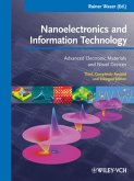
A comprehensive advanced level examination of the transport theory of nanoscale devices _ Provides advanced level material of electron transport in nanoscale devices from basic principles of quantum mechanics through to advanced theory and various numerical techniques for electron transport _ Combines several up-to-date theoretical and numerical approaches in a unified manner, such as Wigner-Boltzmann equation, the recent progress of carrier transport research for nanoscale MOS transistors, and quantum correction approximations _ The authors approach the subject in a logical and systematic…mehr
Andere Kunden interessierten sich auch für
![Mos Devices for Low-Voltage and Low-Energy Applications Mos Devices for Low-Voltage and Low-Energy Applications]() Yasuhisa OmuraMos Devices for Low-Voltage and Low-Energy Applications178,99 €
Yasuhisa OmuraMos Devices for Low-Voltage and Low-Energy Applications178,99 €![Signal Processing for Radiation Detectors Signal Processing for Radiation Detectors]() Mohammad NakhostinSignal Processing for Radiation Detectors167,99 €
Mohammad NakhostinSignal Processing for Radiation Detectors167,99 €![Emergent Behavior in Complex Systems Engineering Emergent Behavior in Complex Systems Engineering]() Saurabh MittalEmergent Behavior in Complex Systems Engineering144,99 €
Saurabh MittalEmergent Behavior in Complex Systems Engineering144,99 €![Active Disturbance Rejection Control for Nonlinear Systems Active Disturbance Rejection Control for Nonlinear Systems]() Bao-Zhu GuoActive Disturbance Rejection Control for Nonlinear Systems166,99 €
Bao-Zhu GuoActive Disturbance Rejection Control for Nonlinear Systems166,99 €![Nanoelectronics and Information Technology Nanoelectronics and Information Technology]() Nanoelectronics and Information Technology86,99 €
Nanoelectronics and Information Technology86,99 €![Charge Transport in Disordered Solids with Applications in Electronics Charge Transport in Disordered Solids with Applications in Electronics]() Sergei Baranovski (ed.)Charge Transport in Disordered Solids with Applications in Electronics326,99 €
Sergei Baranovski (ed.)Charge Transport in Disordered Solids with Applications in Electronics326,99 €![From LED to Solid State Lighting From LED to Solid State Lighting]() S. W. Ricky LeeFrom LED to Solid State Lighting153,99 €
S. W. Ricky LeeFrom LED to Solid State Lighting153,99 €-
-
-
A comprehensive advanced level examination of the transport theory of nanoscale devices
_ Provides advanced level material of electron transport in nanoscale devices from basic principles of quantum mechanics through to advanced theory and various numerical techniques for electron transport
_ Combines several up-to-date theoretical and numerical approaches in a unified manner, such as Wigner-Boltzmann equation, the recent progress of carrier transport research for nanoscale MOS transistors, and quantum correction approximations
_ The authors approach the subject in a logical and systematic way, reflecting their extensive teaching and research backgrounds
Hinweis: Dieser Artikel kann nur an eine deutsche Lieferadresse ausgeliefert werden.
Produktdetails
- Produktdetails
- Wiley - IEEE
- Verlag: Wiley & Sons / Wiley-IEEE Press
- Artikelnr. des Verlages: 1W118871660
- 1. Auflage
- Seitenzahl: 450
- Erscheinungstermin: 24. Oktober 2016
- Englisch
- Abmessung: 244mm x 170mm x 18mm
- Gewicht: 544g
- ISBN-13: 9781118871669
- ISBN-10: 1118871669
- Artikelnr.: 44829214
- Herstellerkennzeichnung
- Produktsicherheitsverantwortliche/r
- Europaallee 1
- 36244 Bad Hersfeld
- gpsr@libri.de
Hideaki Tsuchiya, Associate Professor, Kobe University, Japan. Professor Tsuchiya received his Ph. D in electronic engineering from Kobe University, Kobe, Japan, in 1993. He has lectured for over ten years to graduate students on the Advanced Theory of Integrated Nanoscale Devices. His research interests focus on quantum transport simulation and atomistic modeling of nanoscale devices. He has co-written over 100 journals articles and Proceedings. Yoshinari Kamakura, Associate Professor, Department of Electrical, Electronic and Information Engineering, Graduate School of Engineering, Osaka University, Japan. Professor Kamakura obtained his PhD from Osaka University in 1994 and has worked in various roles at the same institution. His research interests include semiconductor device engineering and he has co-authored a number of journals articles on the subject. He is a member of the IEEE.
Preface ix
Acknowledgements xi
1 Emerging Technologies 1
1.1 Moore's Law and the Power Crisis 1
1.2 Novel Device Architectures 2
1.3 High Mobility Channel Materials 5
1.4 Two?-Dimensional (2?-D) Materials 7
1.5 Atomistic Modeling 8
2 First?-principles calculations for Si nanostructures 12
2.1 Band structure calculations 12
2.1.1 Si ultrathin?-body structures 12
2.1.2 Si nanowires 17
2.1.3 Strain effects on band structures: From bulk to nanowire 20
2.2 Tunneling current calculations through Si/SiO2/Si structures 31
2.2.1 Atomic models of Si (001)/SiO2 /Si (001) structures 32
2.2.2 Current?-voltage characteristics 33
2.2.3 SiO2 thickness dependences 35
3 Quasi?-ballistic Transport in Si Nanoscale MOSFETs 41
3.1 A picture of quasi?-ballistic transport simulated using quantum?-corrected Monte Carlo simulation 41
3.1.1 Device structure and simulation method 42
3.1.2 Scattering rates for 3?-D electron gas 44
3.1.3 Ballistic transport limit 46
3.1.4 Quasi?-ballistic transport 50
3.1.5 Role of elastic and inelastic phonon scattering 51
3.2 Multi?-sub?-band Monte Carlo simulation considering quantum confinement in inversion layers 55
3.2.1 Scattering Rates for 2?-D Electron Gas 56
3.2.2 Increase in Dac for SOI MOSFETs 58
3.2.3 Simulated electron mobilities in bulk Si and SOI MOSFETs 59
3.2.4 Electrical characteristics of Si DG?-MOSFETs 61
3.3 Extraction of quasi?-ballistic transport parameters in Si DG?-MOSFETs 64
3.3.1 Backscattering coefficient 64
3.3.2 Current drive 66
3.3.3 Gate and drain bias dependences 67
3.4 Quasi?-ballistic transport in Si junctionless transistors 69
3.4.1 Device structure and simulation conditions 70
3.4.2 Influence of SR scattering 71
3.4.3 Influence of II scattering 74
3.4.4 Backscattering coefficient 75
3.5 Quasi?-ballistic transport in GAA?-Si nanowire MOSFETs 76
3.5.1 Device structure and 3DMSB?-MC method 76
3.5.2 Scattering rates for 1?-D electron gas 77
3.5.3 ID-VG characteristics and backscattering coefficient 79
4 Phonon Transport in Si Nanostructures 85
4.1 Monte Carlo simulation method 87
4.1.1 Phonon dispersion model 87
4.1.2 Particle simulation of phonon transport 88
4.1.3 Free flight and scattering 89
4.2 Simulation of thermal conductivity 91
4.2.1 Thermal conductivity of bulk silicon 91
4.2.2 Thermal conductivity of silicon thin films 94
4.2.3 Thermal conductivity of silicon nanowires 98
4.2.4 Discussion on Boundary scattering effect 100
4.3 Simulation of heat conduction in devices 102
4.3.1 Simulation method 102
4.3.2 Simple 1?-D structure 103
4.3.3 FinFET structure 106
5 Carrier Transport in High?-mobility MOSFETs 112
5.1 Quantum?-corrected MC Simulation of High?-mobility MOSFETs 112
5.1.1 Device Structure and Band Structures of Materials 112
5.1.2 Band Parameters of Si, Ge, and III?-V Semiconductors 114
5.1.3 Polar?-optical Phonon (POP) Scattering in III?-V Semiconductors 115
5.1.4 Advantage of UTB Structure 116
5.1.5 Drive Current of III?-V, Ge and Si n?-MOSFETs 119
5.2 Source?-drain Direct Tunneling in Ultrascaled MOSFETs 124
5.3 Wigner Monte Carlo (WMC) Method 125
5.3.1 Wigner Transport Formalism 126
5.3.2 Relation with Quantum?-corrected MC Metho

